Balancing Layers in Your PCB Layout
By A Mystery Man Writer
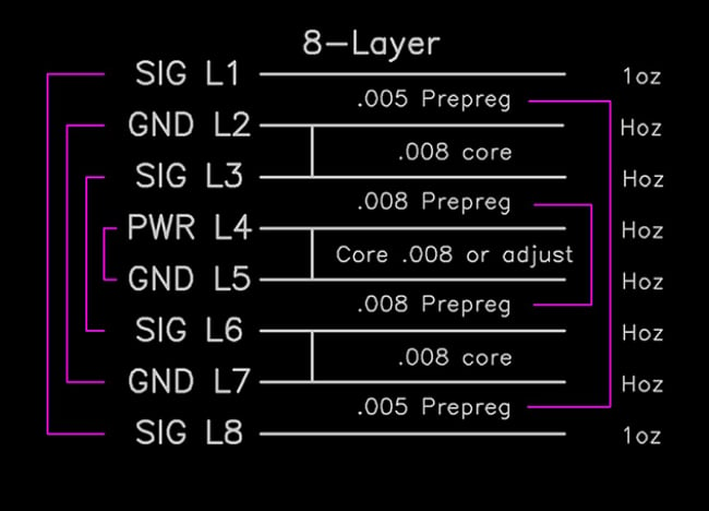
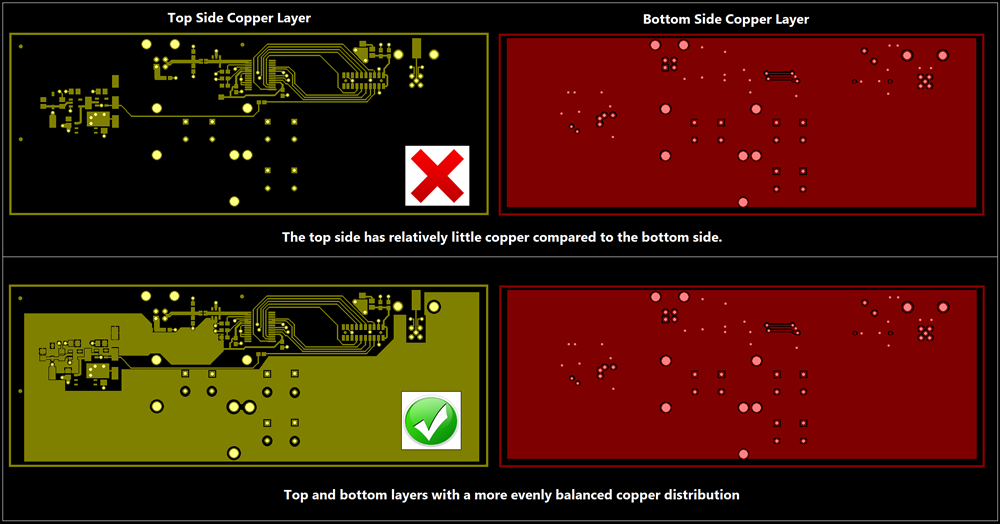
Balancing layers in your PCB layout stack-up, which both layer surfaces and cross-sectional structure of the circuit board are reasonably symmetrical.
Minimizing Bow and Twist

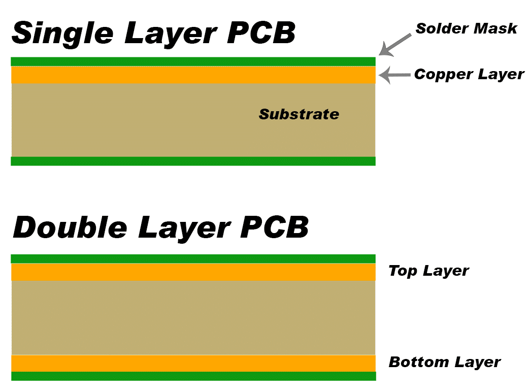
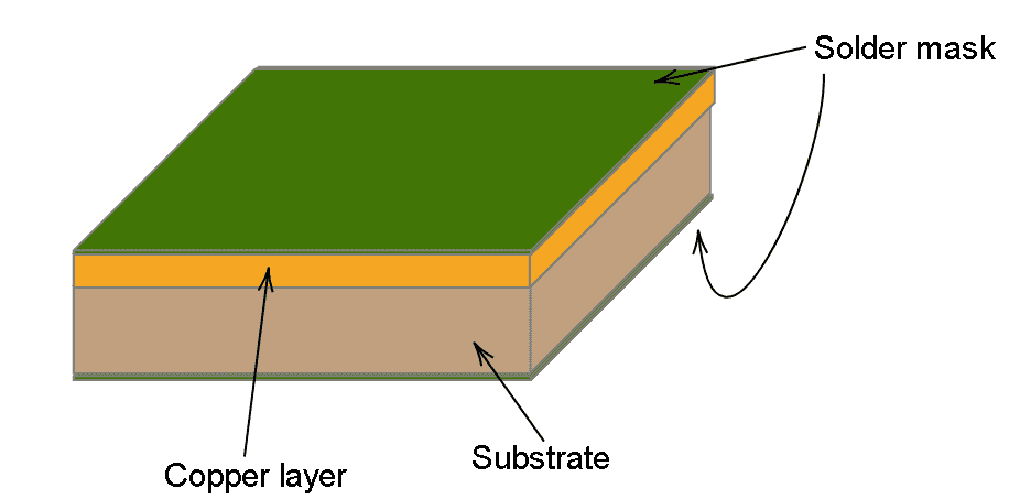
PCB Layers: Everything You Need to Know
Epec's Blog Printed Circuit Boards (7)
The Importance of PCB Trace Widths in PCB Design
How to Design a PCB Layout - Circuit Basics

Balancing Layers in Your PCB Layout

Controlled Impedance Requirements, PCB Impedance

Epec's Blog Printed Circuit Boards (7)

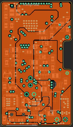
DIY-Self-Balancing-Robot-With-Custom-PCB, Details
An Overview of Layer Stack Management in PCB Design

Balanced and unbalanced PCB layer stack-up for controlling radiated emissions

4 Layer PCB Layout Tutorial,Stack-up design,and Cost of manufacturing - RAYPCB

Understanding PCB Thickness: A Comprehensive Guide
Best Practices for Designing a PCB Layout - Circuit Basics

PCB Layers Explained: Everything You Need to Know